Demand keeps climbing
Hyperscale AI data center bandwidth and power demand keep rising, and optical interconnect is moving closer to the chip.
Upgrade the collimation layer. Keep the proven fiber-array platform.
OneOQ designs flat nano-optics on fused silica for the collimation and coupling layer inside fiber arrays, built for the 1310 nm O-band and for optical interconnect and optical I/O in silicon photonics.
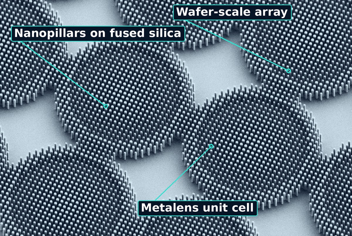
Hyperscale AI data center bandwidth and power demand keep rising, and optical interconnect is moving closer to the chip.
In co-packaged optics (CPO) and near-package optics, the density, alignment and cost of the fiber array interface become first-order constraints for optical I/O.
Multi-channel fiber arrays need every channel collimated accurately at 1310 nm, across a whole array, at volume.
The metalens array (MLA) is a flat, lithographically defined nano-optics layer on fused silica. It drops into the collimation and coupling layer of a fiber array, so the fiber-array platform stays and only the collimation layer is upgraded for silicon photonics and co-packaged optics.
| Substrate | Fused silica |
| Pitch | 0.100 to 0.500 mm range |
| Format | Wafer or diced parts, in standard formats (e.g. 12.7 mm diced dies) |
| Coating | AR-coated |
| Design wavelength | 1310 nm (O-band) and 1550 nm band (C-band) |
| Samples | Targeted Q1 2027 |
Engineering-sample targets. Qualification data to follow.
Growing hyperscale clusters multiply the number of optical links that have to be built and aligned.
Co-packaged and near-package optics put the fiber array interface right beside the silicon photonics chip.
A flat, single-mask, dicing-friendly, wafer-scale metalens layer is built to scale like a semiconductor part.
A scroll through the OneOQ poster series, from the physics of fiber attach to where the optical interconnect market is heading.
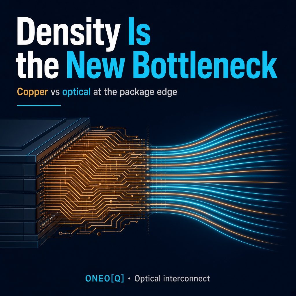
AI packages keep packing more compute into the same shoreline, so copper lanes hit density and loss walls at the package edge. Optical I/O raises bandwidth per millimeter of edge without the same SerDes tax, which is why density—not raw FLOPs—is becoming the constraint that matters.
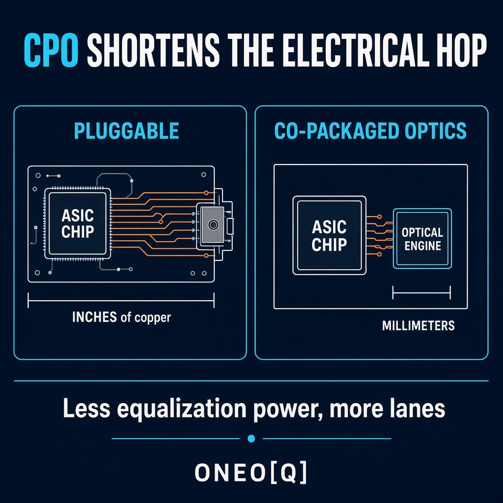
Traditional pluggables force high-speed electrical signals across inches of PCB before light takes over. Co-packaged optics shrink that hop to millimeters next to the ASIC, cutting equalization power and freeing lane count to scale.
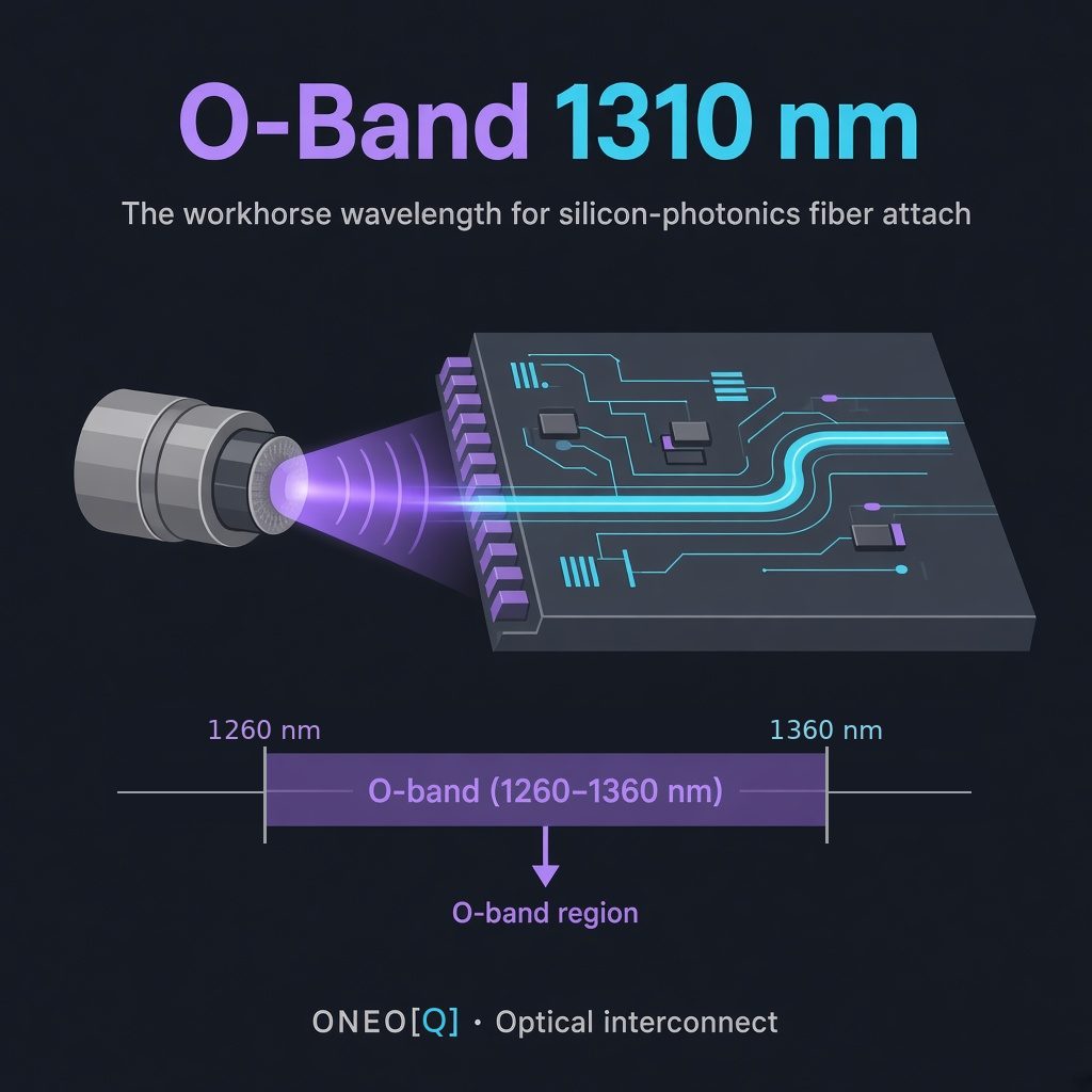
Inside datacenters, silicon photonics usually couples in the O-band near 1310 nm, where standard single-mode fiber has near-zero chromatic dispersion. That band choice drives fiber-attach design: mode field, collimation optics, and the tolerances you can hold in volume.
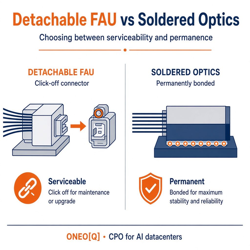
Permanent optical bonds can look simpler on day one, but they make every fiber or connector failure a package-level event. A detachable fiber-array unit keeps the optical path serviceable so ops can replace fiber without scrapping the whole engine.
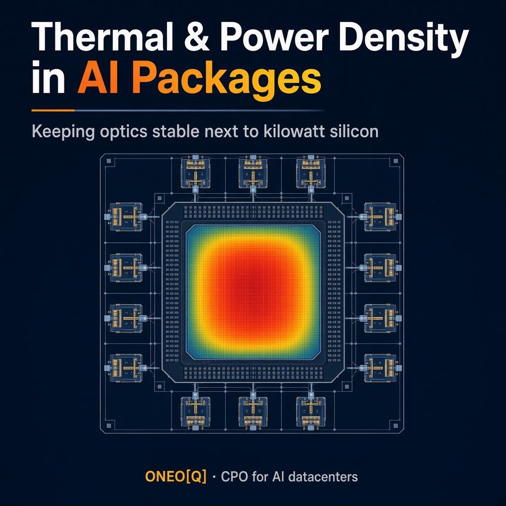
Kilowatt-class accelerators put optics in a harsh thermal neighborhood where alignment and reliability still have to hold. CPO only works if the optical path stays stable while the silicon next door dumps heat.
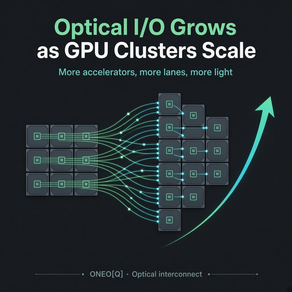
Bigger training and inference clusters multiply links between GPUs, switches, and racks. Optical lane count scales with that fabric, so interconnect density has to grow as fast as the compute graph.
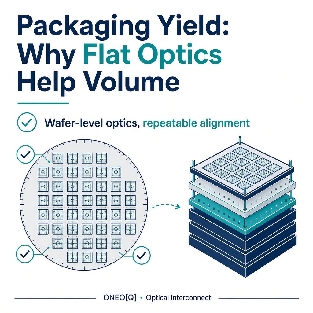
Discrete micro-optics are hard to place repeatably at the counts AI packages need. Flat, wafer-processed optics bring lithographic consistency to collimation and coupling, which is how you protect packaging yield at volume.
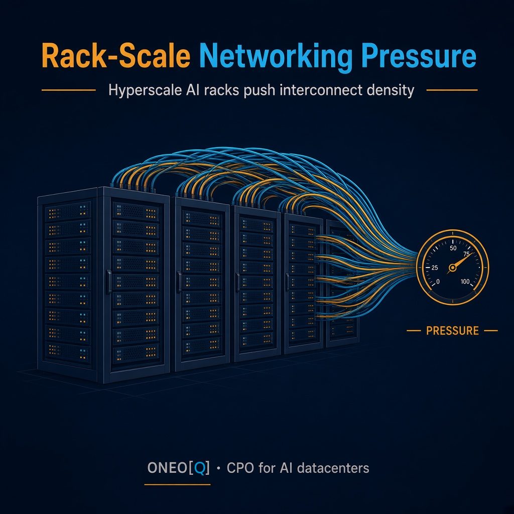
Hyperscale AI racks pack more bandwidth into fixed power, cooling, and faceplate budgets. That pressure pushes interconnect toward shorter electrical reaches and denser optical ports at the rack and package.
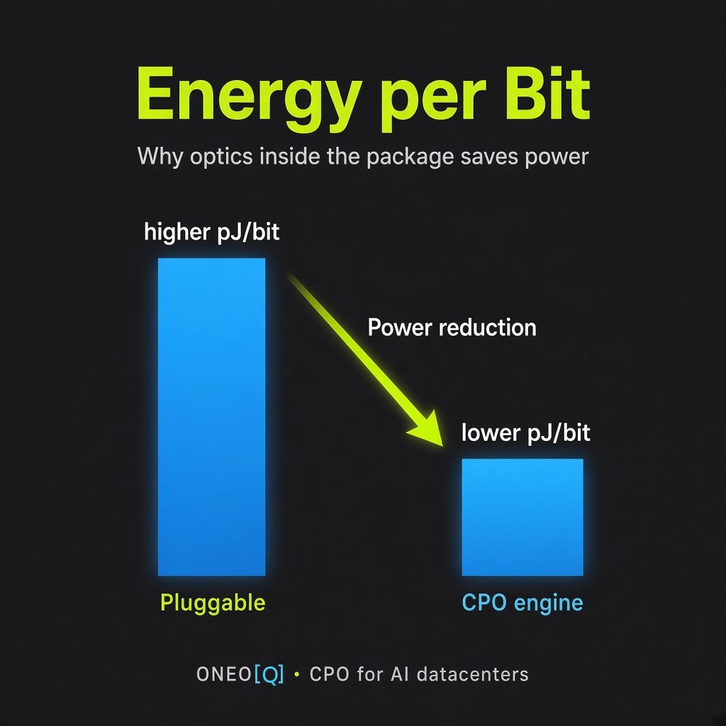
Moving the E/O conversion closer to the ASIC cuts the power burned in long electrical SerDes hops. At AI scale, picojoules per bit at the package edge are as strategic as FLOPs per watt on the die.
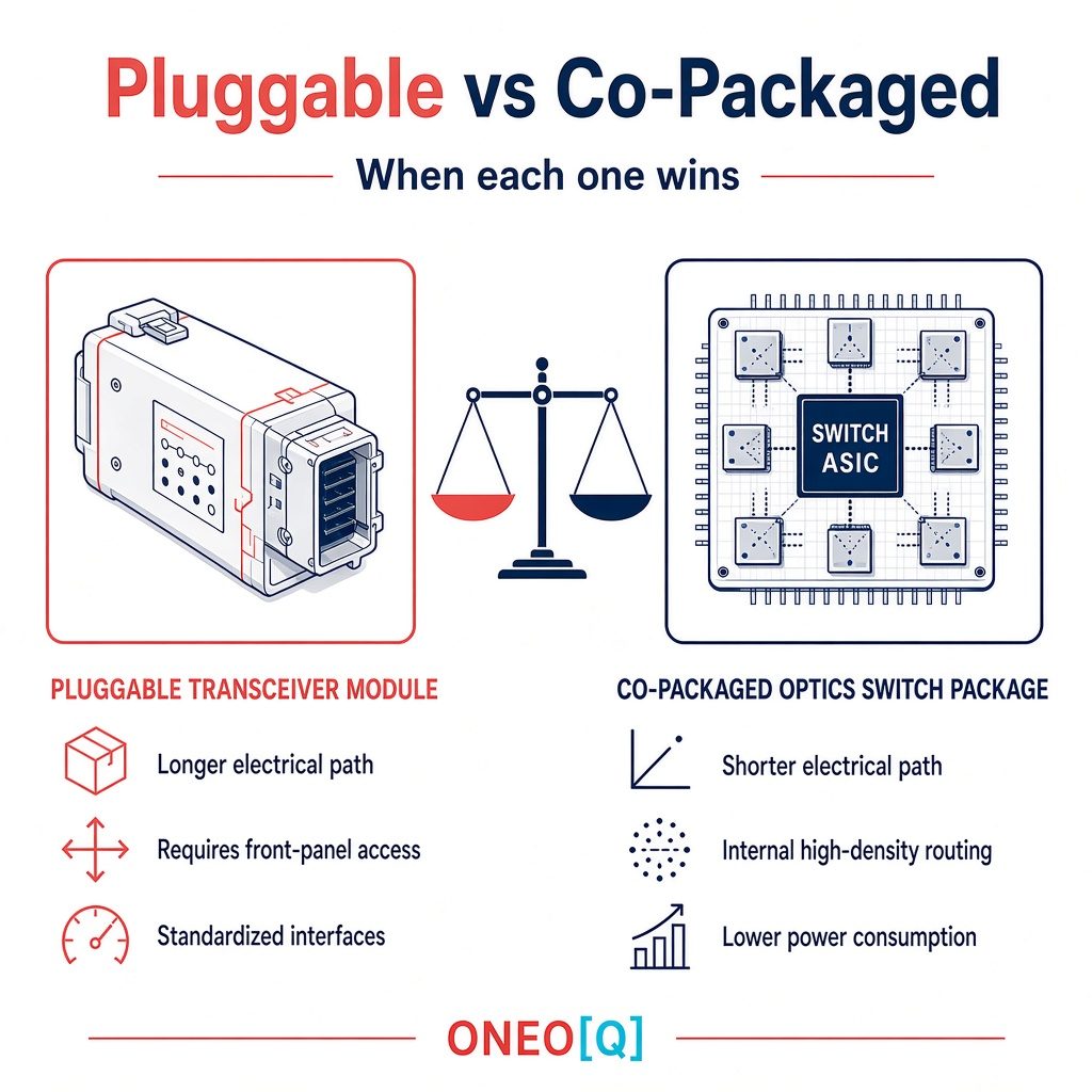
Pluggables win when you need field replaceability and flexible reach options. CPO wins when density and energy per bit dominate—and many AI systems will mix both where each is strongest.
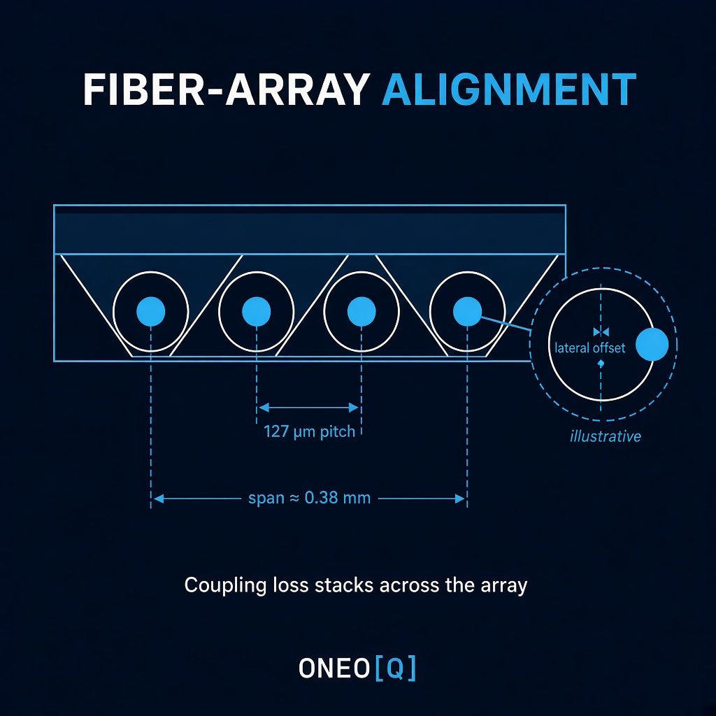
Multi-fiber attach lives or dies on micron-level lateral and angular alignment. Coupling loss stacks across the array, so the collimation layer has to be designed for the tolerance budget you can actually manufacture.
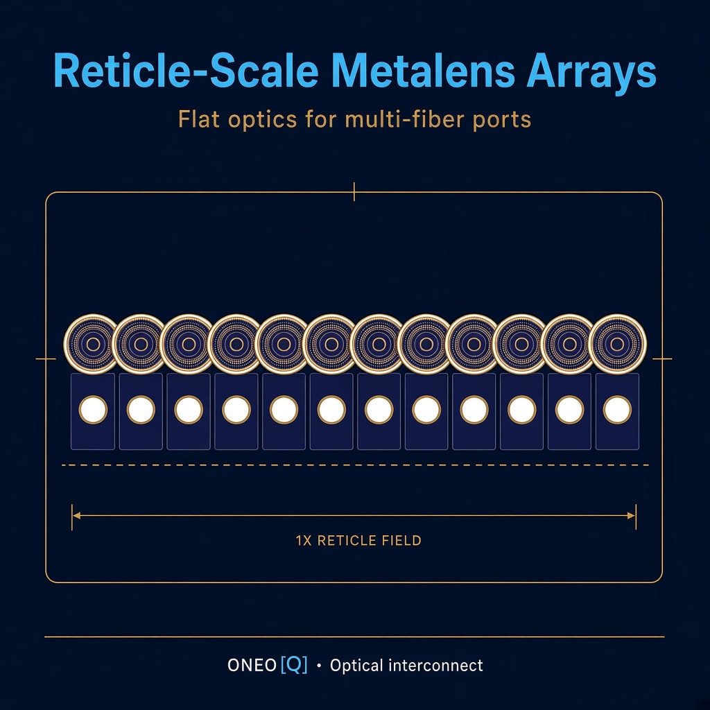
A fiber array needs a matching array of collimation elements, not one lens at a time. Reticle-scale metalens arrays print that pattern in one wafer process, sized to the port pitch of the FAU.
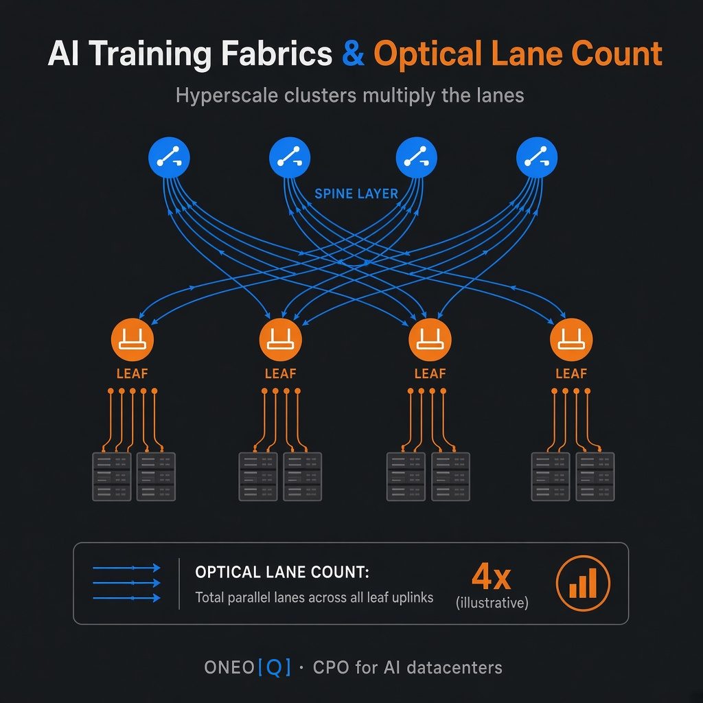
Large training fabrics add optical lanes at every hop—GPU to switch, leaf to spine, rack to rack. Lane count becomes a first-class architecture variable, not an afterthought of copper SI.
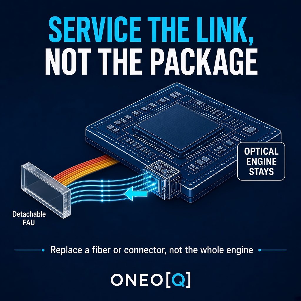
In production AI clusters, the expensive failure mode is replacing a whole optical engine for a fiber or connector fault. Detachable attach keeps optics maintainable so operators can service the link, not the package.
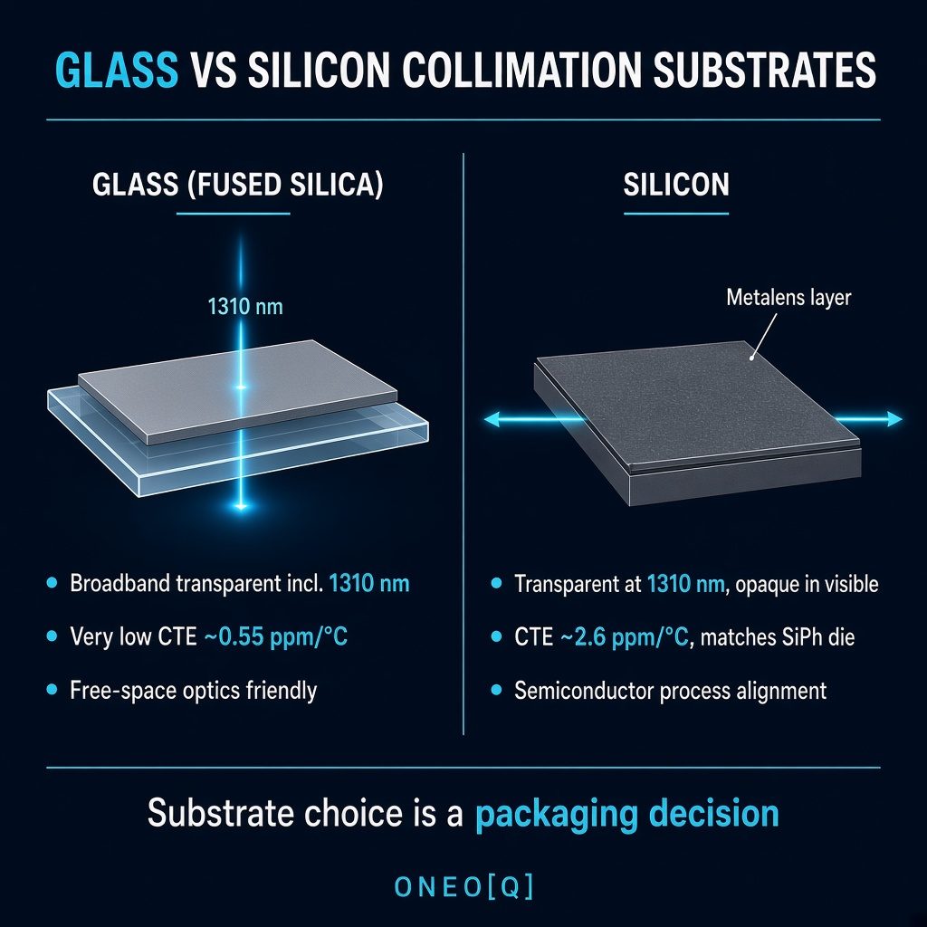
Glass offers broadband transparency and familiar optical CTE behavior for free-space coupling paths; silicon brings semiconductor process alignment but different thermal and transparency trade-offs. Collimation-layer substrate choice is a packaging decision as much as an optics one.
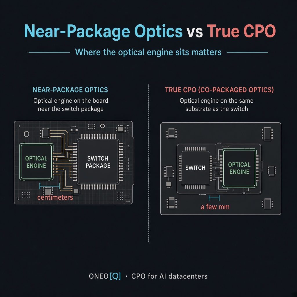
Near-package optics sit close to the ASIC but still off the main package substrate; true CPO co-packages the optical engine with the silicon. Where the engine sits changes reach, power, thermal load, and how dense the fiber attach can be.
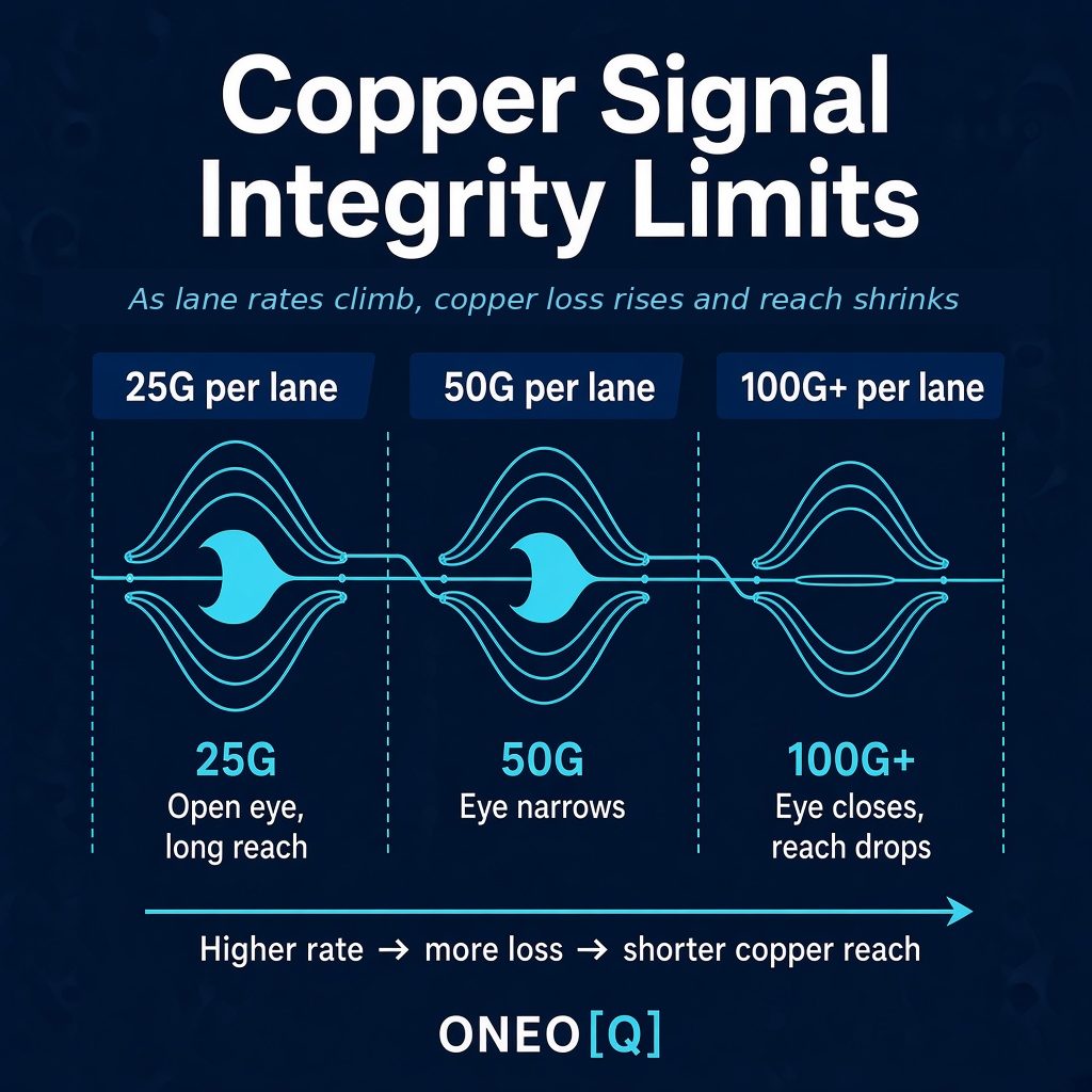
At 100G+ per lane, copper loss, crosstalk, and equalization budgets shrink the usable electrical reach fast. That is the physics pushing high-radix AI systems to put optics earlier in the path.
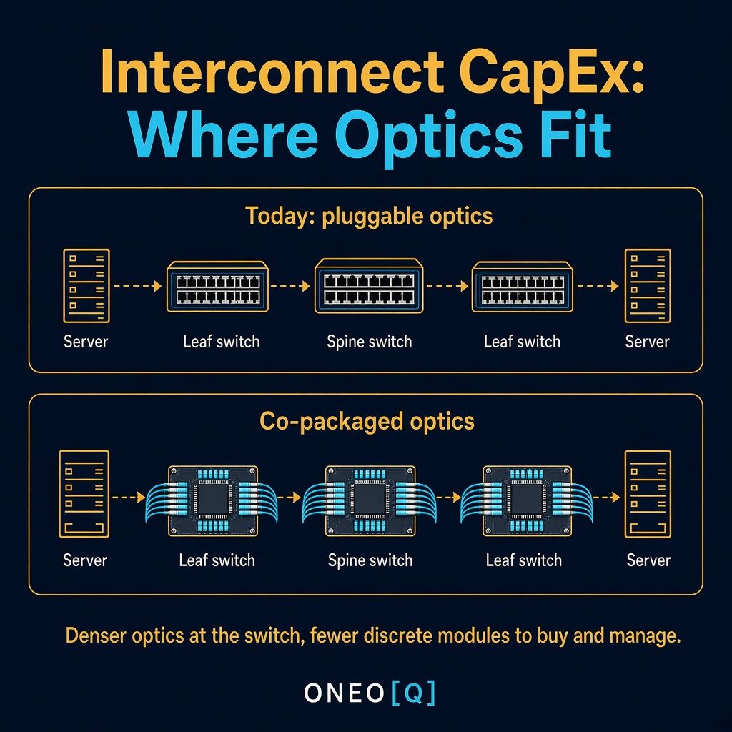
Hyperscalers pay for every switch hop, cable, and watt in the fabric. Fewer electrical hops and denser optical ports cut network CapEx and OpEx even when the optical engines themselves look expensive on paper.
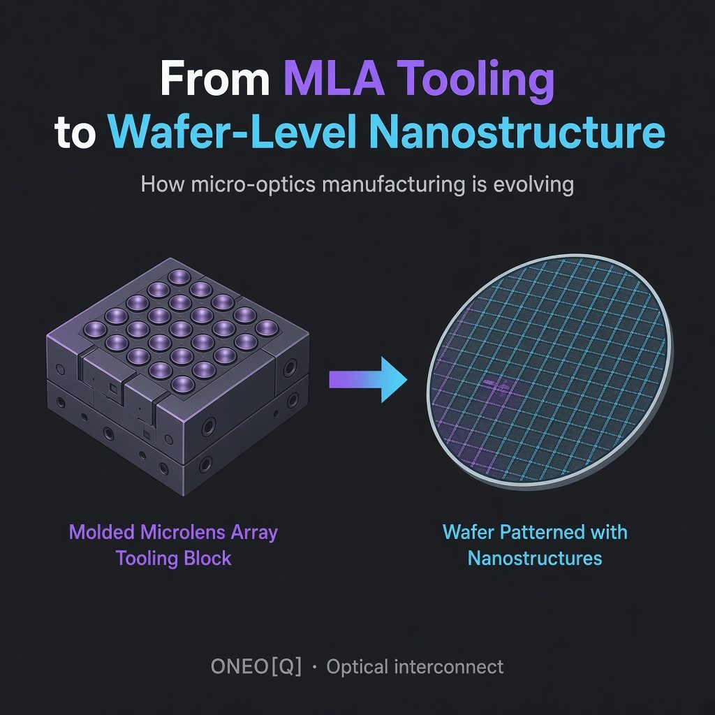
Classic microlens arrays lean on molding and discrete tooling that struggle at AI port counts. Wafer-level nanostructures move collimation into a semiconductor-like process so multi-fiber optics can scale with the package.
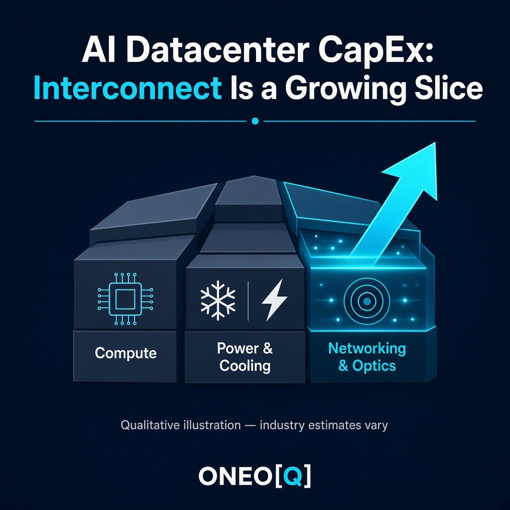
AI datacenter budgets still go mostly to compute, but networking and optics take a bigger share as clusters grow. Every added accelerator brings more links, so interconnect grows into a strategic line item.
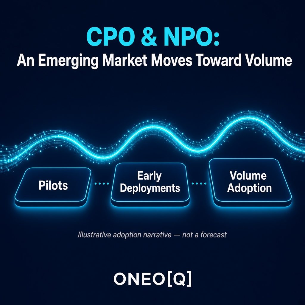
Co-packaged and near-package optics are moving from pilots toward early deployments as AI systems hit electrical I/O limits. How fast they reach volume depends on packaging maturity, serviceability, and supply-chain readiness as much as on the physics.
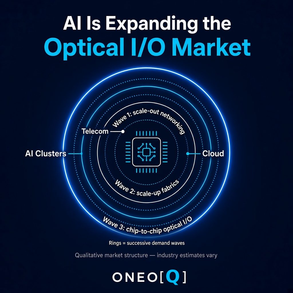
Optical interconnect grew up serving telecom and then cloud, and AI clusters are now its fastest-growing frontier. Each new tier of demand needs more bandwidth per link and many more links.
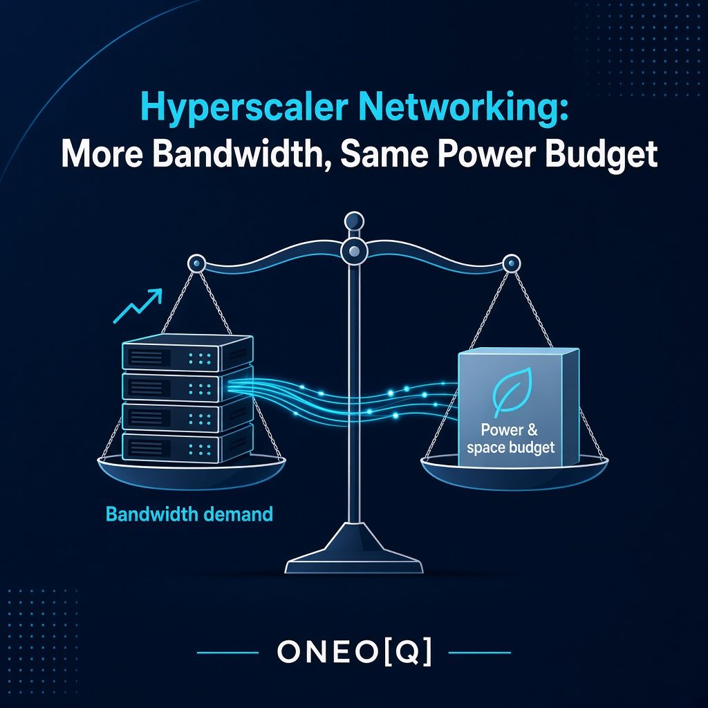
Hyperscale operators keep needing more bandwidth while their power, cooling, and space budgets stay roughly fixed. That squeeze favors interconnect that delivers more bits per watt and per unit of faceplate.
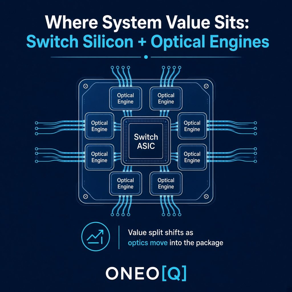
In a co-packaged switch, value is shared between the switch ASIC and the optical engines around it. As optics move into the package, more of the system's value and engineering moves to the package edge.
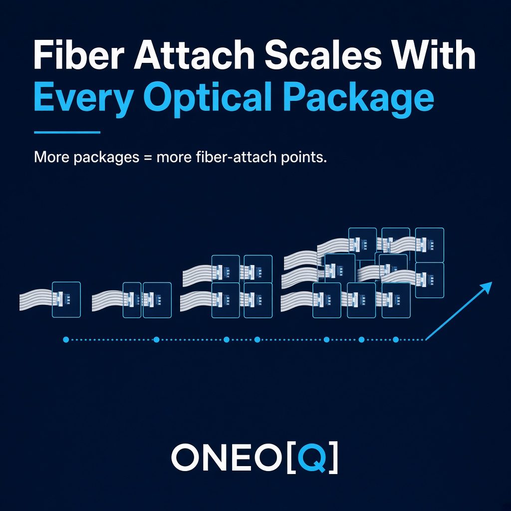
Every optical engine needs a precise, reliable fiber connection, so attach volume grows with each package shipped. Fiber attach that is manufacturable and serviceable at scale becomes a market in its own right.
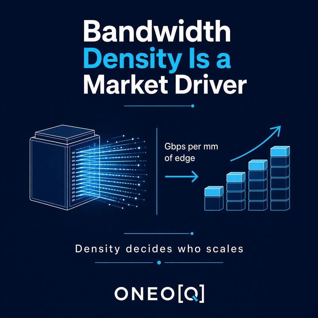
Bandwidth per millimeter of package edge isn't just an engineering metric. It sets how far an AI system can scale, so the technologies that raise density decide where market value goes.
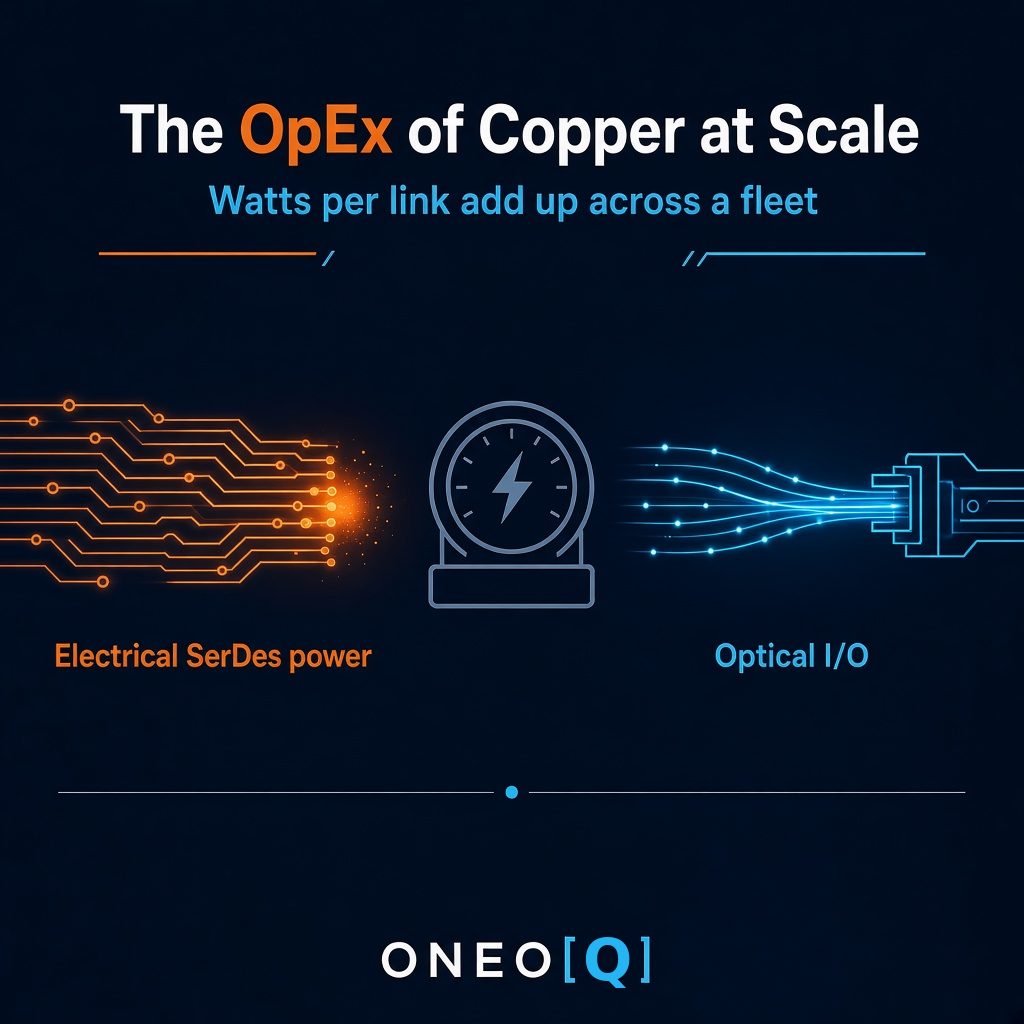
Electrical SerDes power looks small per link, but across a fleet of many thousands of links it becomes a real operating cost. Cutting energy per bit with optical I/O lowers the bill for power and cooling over the system's life.
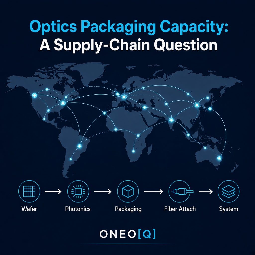
The path from wafer to photonics, packaging, fiber attach, and finished system runs across a global supply chain. Packaging and attach capacity may limit how fast optical interconnect can scale, as much as demand does.
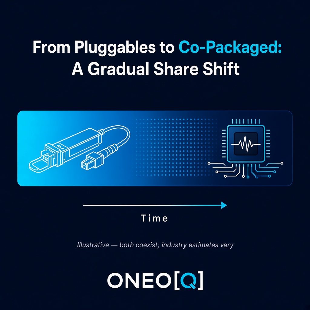
Pluggable transceivers remain the workhorse today, and co-packaged optics are expected to take share gradually where density and power matter most. Both will coexist for years, and the mix is likely to shift step by step, not all at once.
Founder & CEO, OneOQ LLC
Team of five: one full-time and four part-time.
ceo@oneoq.com
oneoq.com
Fishers, Indiana